Product Summary
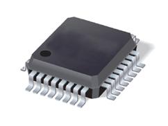
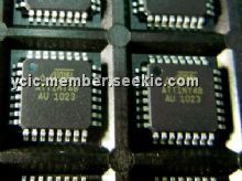
The ATTINY48-AU is a low-power CMOS 8-bit microcontroller based on the AVR enhanced RISC architecture. By executing powerful instructions ina single clock cycle, the ATTINY48-AU achieves throughputs approaching 1 MIPS per MHz allowing the system designer to optimize power con-sumption versus processing speed.
Parametrics
ATTINY48-AU absolute maximum ratings: (1)Operating Temperature: -55℃ to +125℃; (2)Storage Temperature: -65℃ to +150℃; (3)Voltage on any Pin except RESET; (4)with respect to Ground: -0.5V to VCC +0.5V; (5)Voltage on RESET with respect to Ground: -0.5V to +13.0V; (6)Maximum Operating Voltage: 6.0V; (7)DC Current per I/O Pin: 40.0 mA; (8)DC Current VCCand GND Pins: 200.0 mA.
Features
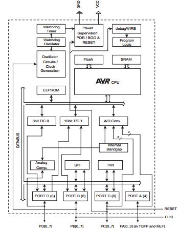
ATTINY48-AU features: (1)High Performance, Low Power AVR 8-Bit Microcontroller; (2)Advanced RISC Architecture, 123 Powerful Instructions – Most Single Clock Cycle Execution, 32 x 8 General Purpose Working Registers; Fully Static Operation; (3)High Endurance Non-volatile Memory Segments, 4K/8K Bytes of In-System Self-Programmable Flash program memory(ATtiny48/88); 64/64 Bytes EEPROM (ATtiny48/88); 256/512 Bytes Internal SRAM (ATtiny48/88); Write/Erase Cycles: 10,000 Flash/100,000 EEPROM; Data retention: 20 years at 85℃/100 years at 25℃; Optional Boot Code Section with Indepentent Lock Bits; (4)In-System Programming by On-chip Boot Program; (5)True Read-While-Write Operation, Programming Lock for Software Security; (6)Peripheral Features, One 8-bit Timer/Counter with Separate Prescaler and Compare Mode; One 16-bit Timer/Counter with Prescaler, and Compare and Capture Modes; 8-channel 10-bit ADC in 32-lead TQFP and 32-pad QFN/MLF package; 6-channel 10-bit ADC in 28-pin PDIP and 28-pad QFN/MLF package; Master/Slave SPI Serial Interface; Byte-oriented 2-wire Serial Interface (Philips I2C Compatible); Programmable Watchdog Timer with Separate On-chip Oscillator; On-chip Analog Comparator; Interrupt and Wake-up on Pin Change; (7)Special Microcontroller Features, debugWIRE On-chip Debug System; In-System Programmable via SPI Port; Power-on Reset and Programmable Brown-out Detection; Internal Calibrated Oscillator; External and Internal Interrupt Sources; Three Sleep Modes: Idle, ADC Noise Reduction and Power-down; (8)I/O and Packages, 28 Programmable I/O Lines in 32-lead TQFP and 32-pad QFN/MLF package; 24 Programmable I/O Lines in 28-pinPDIP and 28-pad QFN/MLF package; 28-pin PDIP, 32-lead TQFP, 28-pad QFN/MLF and 32-pad QFN/MLF; (9)Operating Voltage: 1.8– 5.5V; (10)Temperature Range: -40℃ to +85℃; (11)Speed Grade: 0– 2 MHz @ 1.8 to 5.5V; 0– 6 MHz @ 2.7 to 5.5V; 0 to 12 MHz @ 4.5– 5.5V; (12)Low Power Consumption, Active Mode: 1 MHz, 1.8V: 240μA; Power-down Mode: 0.1μA at 1.8V.
Diagrams

| Image | Part No | Mfg | Description |  |
Pricing (USD) |
Quantity | ||||||||||||
|---|---|---|---|---|---|---|---|---|---|---|---|---|---|---|---|---|---|---|
 |
 ATTINY48-AU |
 Atmel |
 8-bit Microcontrollers (MCU) 4KB In-system Flash 12MHz 1.8V-5.5V |
 Data Sheet |

|
|
||||||||||||
 |
 ATTINY48-AUR |
 Atmel |
 8-bit Microcontrollers (MCU) AVR 4KB FLSH 64B EE 256B SRAM-12MHz, IND |
 Data Sheet |

|
|
||||||||||||
 (China (Mainland))


