(China (Mainland))

Product Summary
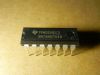
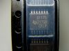
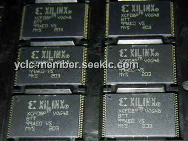
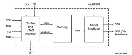
The XCF08PV048C is a Platform Flash in-system programmable configuration PROM. Available in 1 to 32 Megabit (Mbit) densities, the PROM provides an easy-to-use, cost-effective, and reprogrammable method for storing large Xilinx FPGA configuration bitstreams. The XCF08PV048C supports Master Serial and Slave Serial FPGA configuration modes.
Parametrics
XCF08PV048C absolute maximum ratings: (1)Internal supply voltage relative to GND, VCCINT: -0.5 to +2.7 V; (2)I/O supply voltage relative to GND, VCCO: -0.5 to +4.0 V; (3)JTAG I/O supply voltage relative to GND, VCCJ: -0.5 to +4.0 V; (4)Input voltage with respect to GND, VCCO <2.5V, VIN: -0.5 to +3.6V; VCCO ≥2.5V, VIN: -0.5 to +3.6 V; (5)Voltage applied to High-Z output, VCCO <2.5V, VTS: -0.5 to +3.6V; VCCO ≥2.5V, VTS: -0.5 to +3.6 V; (6)Storage temperature (ambient), TSTG: -65 to +150℃; (7)Junction temperature, TJ: +125℃.
Features
XCF08PV048C features: (1)In-System Programmable PROMs for Configuration of Xilinx FPGAs; (2)Low-Power Advanced CMOS NOR FLASH Process; (3)Endurance of 20,000 Program/Erase Cycles; (4)Operation over Full Industrial Temperature Range (-40℃ to +85℃); (5)IEEE Standard 1149.1/1532 Boundary-Scan (JTAG) Support for Programming, Prototyping, and Testing; (6)JTAG Command Initiation of Standard FPGA Configuration; (7)Cascadable for Storing Longer or Multiple Bitstreams; (8)Dedicated Boundary-Scan (JTAG) I/O Power Supply (VCCJ); (9)I/O Pins Compatible with Voltage Levels Ranging From 1.5V to 3.3V; (10)Design Support Using the Xilinx Alliance ISE and Foundation ISE Series Software Packages.
Diagrams
 |
 XCF01S |
Other |
|
Data Sheet |
Negotiable |
|
||||
|
XCF02S |
Other |
|
Data Sheet |
Negotiable |
|
||||
|
XCF02SVOG20C |
Other |
|
Data Sheet |
Negotiable |
|
||||
|
XCF04S |
Other |
|
Data Sheet |
Negotiable |
|
||||
|
XCF04SVO20C |
Other |
|
Data Sheet |
Negotiable |
|
||||
|
XCF04SVOG20C |
Other |
|
Data Sheet |
Negotiable |
|
||||